Pull to refresh
453.29

Manufacture and development of electronics *

How to establish a process

Show first
Rating limit
Level of difficulty

System-on-Chip bus: AXI4 simplified and explained

Reading time 20 min
Views 27K

Protocol AXI4 was developed for High-bandwidth and low latency applications. It is designed to allow communication between master and slave devices. Master is typically a DMA or CPU and slaves are DRAM controllers, or other specific protocol controllers: UART, SPI, and others. Sometimes one component can implement multiple instances of this protocol. Usually, a prefix is used to differentiate between multiple AXI4 interfaces.

For example, Ethernet MAC can integrate DMA and slave interface used to command MAC. MAC can accept commands on the slave interface that contain data about the location of the next ethernet packet and MAC can start fetching this packet using the separate master interface instance.

This article was motivated by common design mistakes AXI4 designers make when they are designing their Digital IP. (Looking at you Xilinx)

Read more
Total votes 10: ↑10 and ↓0 +10
Comments 1

Common misconceptions about space-grade integrated circuits

Reading time 27 min
Views 21K

Space exploration was always fascinating, and recent developments have reignited the interest to the heights never seen since the last man stood on the Moon. People argue about Mars exploration and features of spaceships as their grandparents would’ve done if the internet existed fifty years ago. I’m an electronics engineer working in the aerospace industry, so I know a thing or two about the technical background of this stuff — and I see that these things aren’t common knowledge, and people often have significantly skewed ideas about the reasons behind many things and decisions. Namely, I’d love to speak of some misconceptions about radiation hardened integrated circuits and the means of protection from radiation-induced damage.

So, let's start our journey
Total votes 15: ↑15 and ↓0 +15
Comments 35

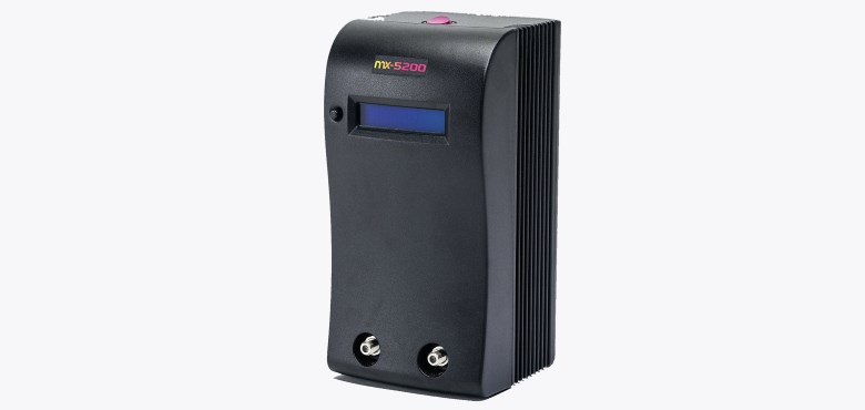
Reverse engineering a high-end soldering station

Reading time 15 min
Views 19K


(This is the translation of the original article performed by baragol)

We had a bunch of photographs of the main PCB, a YouTube video with drain-voltage waveforms of MOSFETs, a forum post with a breakdown of the capacitance values of LC circuit capacitors and also a number of unboxing videos showing the heating-up of the soldering tip. The only thing that really worried me was the video with the measurement of the peak power consumption during the heating-up. There is nothing in the world more helpless and irresponsible and depraved than burned cartridge newly bought for 60 bucks from Amazon. But let me start from the beginning.
Read more →
Total votes 24: ↑23 and ↓1 +22
Comments 1

Physical unclonable functions: protection for electronics against illegal copying

Reading time 7 min
Views 5K

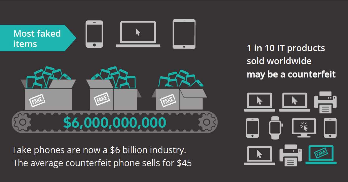
Source: The online counterfeit economy: consumer electronics, a report made by CSC in 2017

Over the past 10 years, the number of fake goods in the world has doubled. This data has been published in the latest Year-End Intellectual Property Rights Review by the US Department of Homeland Security in 2016 (the most current year tracked). A lot of the counterfeiting comes from China (56%), Hong Kong (36%) and Singapore (2%). The manufacturers of original goods suffer serious losses, some of which occur on the electronics market.

Many modern products contain electronic components: clothes, shoes, watches, jewellery, cars.
Last year, direct losses from the illegal copying of consumer electronics and electronic components in the composition of other goods were about $0.5 trillion.

How to solve this problem?
Read more →
Total votes 14: ↑14 and ↓0 +14
Comments 0

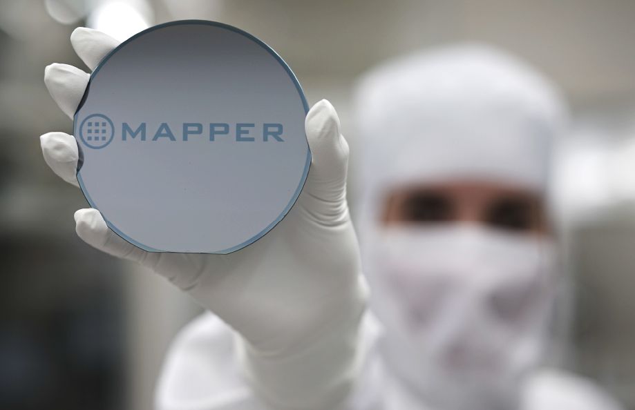
Chemistry lesson: how to expose a microchip's crystal for photography

Reading time 6 min
Views 2K

Introduction


If you have dabbled into microchip photographing before, then this article will probably not offer much to you. But if you want to get into it, but don’t know where to start, then it’s exactly for you.


Before we start, a fair warning: while the procedure is quite entertaining, at first it’ll probably be physically painful. The chemicals used during the process are toxic, so please handle them carefully – that way it’ll still hurt, but less so. Also, if you have even a slight amount of common sense, conduct the procedure in a fully-equipped chemical laboratory under supervision of trained professionals: we’ve had to deal with people who tried to do it at home immediately after reading the guide. And finally: if you don’t know whether you need to pour acid into water or water into acid without a Google search and don’t realize what this lack of knowledge will entail – stop reading this immediately and go to a chemistry 101 course in a local college or something.


Read more →
Total votes 25: ↑24 and ↓1 +23
Comments 0

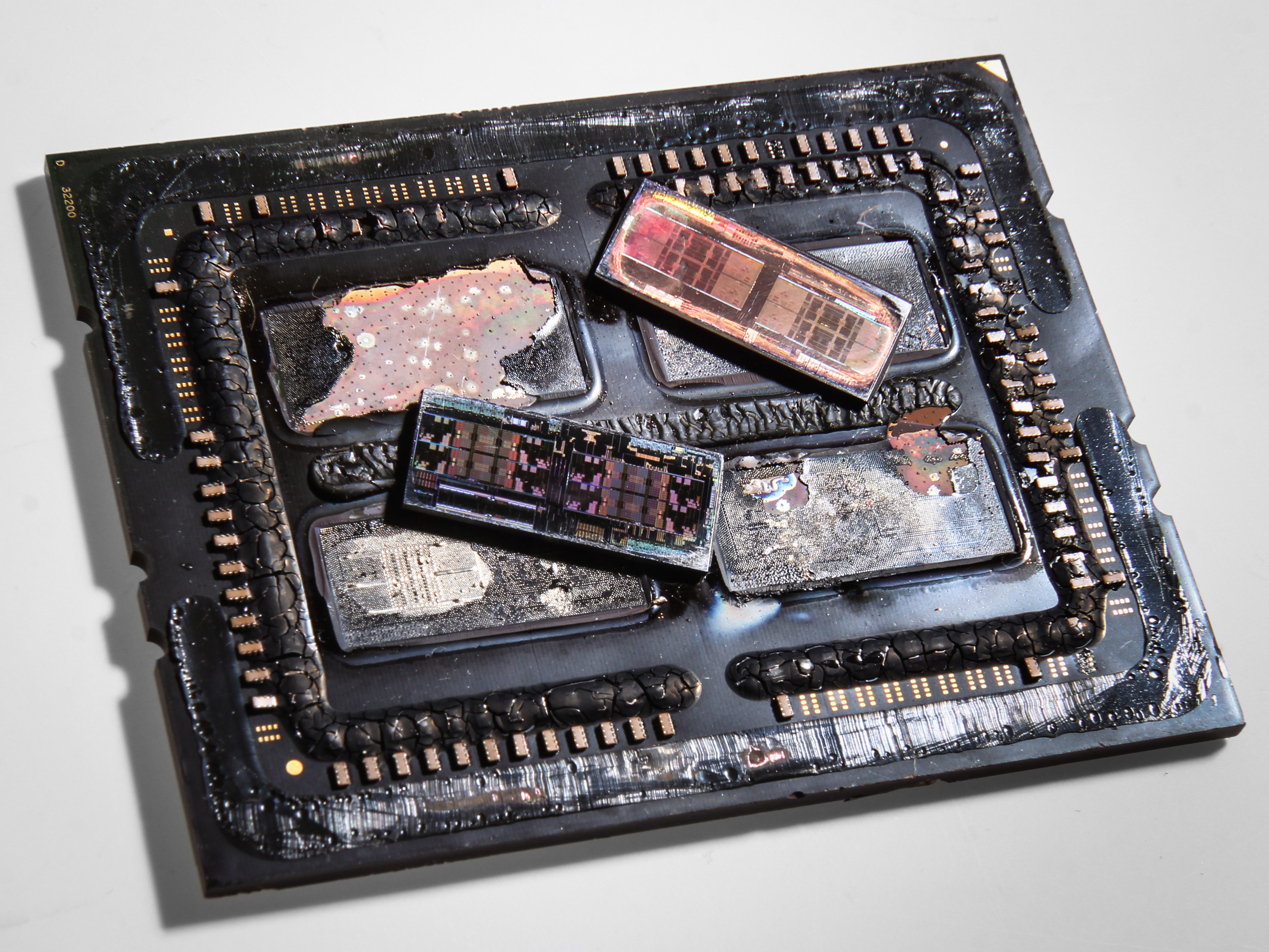
System in Package, or What's Under Chip Package Cover?

Reading time 7 min
Views 5.1K
Transistor feature size is decreasing despite constant rumors about the death of Moore’s law and the fact that industry is really close to physical limits of miniaturisation (or even went through them with some clever technology tricks). Moore’s law, however, created user’s appetite for innovation, which is hard to handle for the industry. That’s why modern microelectronic products aren’t just feature size scaled, but also employ a number of other features, often even more complicated than chip scaling.


Disclaimer: This article is a slightly updated translation of my own piece published on this very site here. If you're Russian-speaking, you may want to check the original. If you're English-speaking, it's worth noting that English is not my native language, so I'll be very grateful for the feedback if you find something weird in the text.
Read more →
Total votes 38: ↑38 and ↓0 +38
Comments 0

Authors' contribution