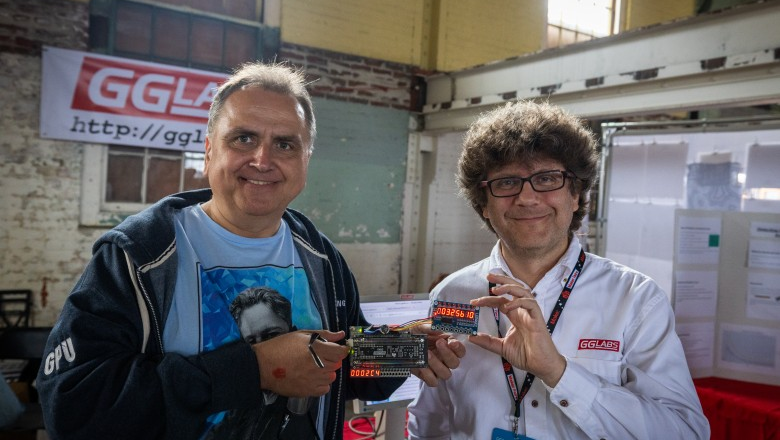
Gowin has clear advantages over Xilinx in the educational FPGA board market: Gowin boards are several times less expensive, the synthesis speed is several times faster, and the EDA package is two orders of magnitude smaller: we are talking about 1G versus 100G disk space. Of course, Xilinx is still the king of high-end prototyping boards that cost $10K-100K, but for the students such boards are irrelevant; such boards are for ASIC design companies. A beginning EE student needs a board for less than $100, and Gowin not only fits the bill but also covers all the needs, specifically:
FPGA *
Programmable logic integrated circuits
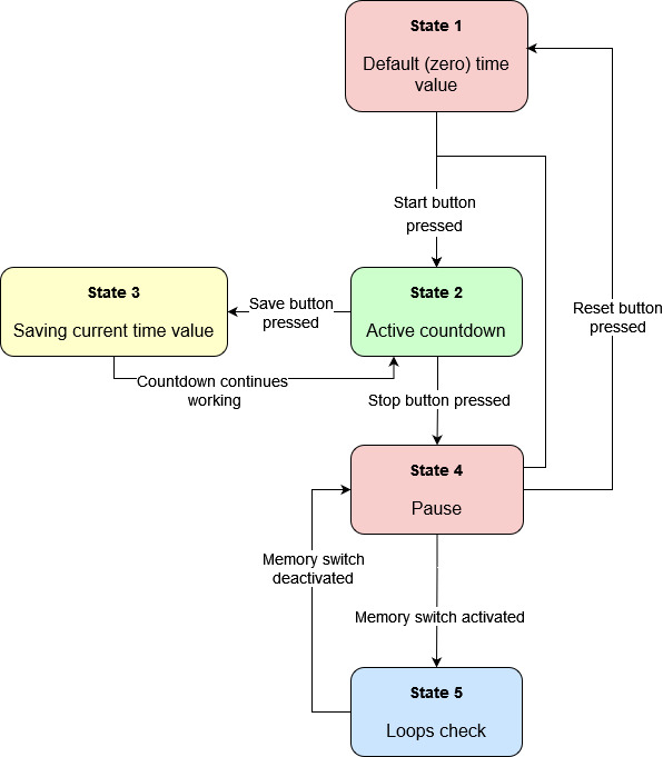
Stopwatch implementation on FPGA board
In this report we describe our implementation experience of a stopwatch system executing on an FPGA board. We programmed this device in the Quartus Prime II software environment by using Verilog hardware description language. The program is tailored to the Altera MAX 10 FPGA board, as well as uses a set of other peripheral devices for progress visualization purposes.
The results of 7 Verilog meetups + the goals and the steps going forward
Since the New Year we had 7 Verilog meetups at HackerDojo. We discussed the modern way of designing digital circuits using hardware description languages, the exercises on FPGA boards and the topic of microarchitecture. For the last two sessions we went over the most basic CPU core that can be used as a baseline for further exercises.
Now, in order to make progress toward the goal of creating new educational materials, it is essential for the regular participants to solve all the homework exercises (see the details in the post below) in parallel with studying the recommended materials.
The next steps are:
1) We are going to do weekly Zoom calls on Sundays, starting March 24, 2024 at 11 am California time (summer time). The link. During this call we are going to discuss the SystemVerilog Homework and the individual projects.
2) Once we develop more materials, we are going to organize a Show-and-Tell session in Hacker Dojo, for a wider audience. During the session several participants from the core team will present demos on various FPGA boards and explain to the curious how FPGA and ASIC work.
Bootstrapping Azerbaijan as a new center of ASIC design + Verilog Meetup #6 in Silicon Valley
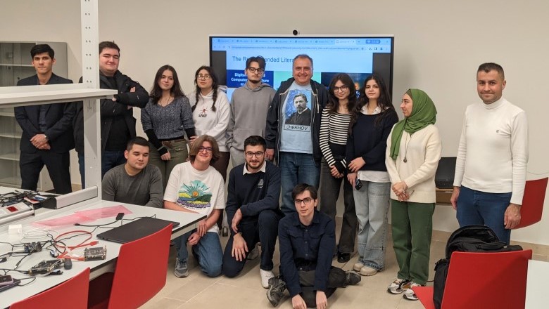
Last week I was doing a seminar on SystemVerilog, ASIC and FPGA at ADA University in Baku, Azerbaijan. I will replicate the last two sessions of this seminar, on RISC-V CPU simulation and synthesis, at the Verilog Meetups on March 3 and March 10 at Hacker Dojo, Mountain View, California. For this reason I am combining the information about Azerbaijan and California seminars in a single post.
First, let's talk about ADA University.
Verilog Meetups @ Hacker Dojo: the status and the plans for 2024
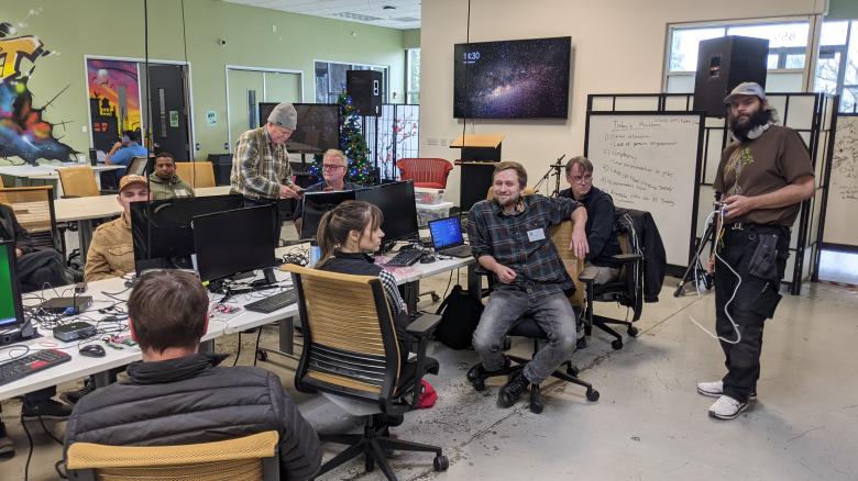
The first meetups of the Portable SystemVerilog Examples group at Hacker Dojo in Mountain View, California were a kind of brainstorming sessions. We discussed the electronic industry, the essence of modern chip design, and the challenges of educating new design engineers. Then we moved to a new mode of action. We started weekly meetings of the core R&D team with the goal to prepare educational materials for the events for a larger audience. The meetings are generally held on Sundays from 11 pm to 2 pm. If you cannot come to Mountain View, you can join online.
We are focusing on interview-level microarchitectural and CPU design examples, providing FPGA vendor-neutral infrastructure and compatibility with open-source ASIC design tools.
Portable SystemVerilog Examples for ASIC and FPGA: the results of the meetup on 2024-01-21 and the next steps
The second meetup of the Portable SystemVerilog Examples group on January 21 2024 at Hacker Dojo in Mountain View, California, went as planned: we moved from the stage of presenting the project to the self-introductions of the participants and the initial tutorial with the first examples. We also started distributing the tasks. The next meetup is tentatively scheduled for January 28 at the same location, from 2 pm to 5 pm. The contents of the meeting will be to work on the examples: basics-graphics-music and systemverilog-homework.
The next steps after a good meetup on Portable SystemVerilog Examples for ASIC and FPGA
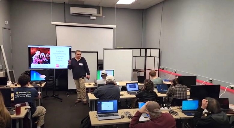
The meetup on January 14 at Hacker Dojo in Mountain View, California, went well, although not as planned - we spent almost all the time talking instead of doing hands-on exercises. The room we booked can fit 30 people and approximately 30 people did show up. The quality of participants was high: approximately half were familiar with hardware description languages and another half came from various software topics. 12 people filled out the questionnaire despite the fact that I forgot to bring 30 pens.
The discussion during and after the presentation was focused and very meaningful: microarchitecture and education, EDA infrastructure / build scripts, open-source ASIC design tools, the economics of ASIC design and manufacturing, high-level synthesis, transaction-level modeling, ASIC prototyping using FPGA boards, FPGA embedded in ASIC (Menta), new FPGA manufacturers (Gowin) and new design languages - Chisel and SpinalHDL.
Four persons came to me after the meeting to discuss their participation in working on open-source portable SystemVerilog examples, and another seven expressed this intention in the questionnaire. So we are meeting again in Hacker Dojo on Sunday, January 21, at 2 PM, this time not in the classroom area, but in the common shared area.
Generally, I am thinking of having regular meetings, probably on a weekly basis for a small team of developers of the educational materials and on a monthly basis for a wider audience, discussing various design and verification topics.
There were two correspondents of Slavic Sacramento who recorded the video of the presentation. They are going to make it available soon.
Why would a software engineer attend an FPGA hardware meetup at Hacker Dojo?
For the last 30 years digital chip design is not a schematic entry anymore: hardware engineers write code just like software engineers.
The difference is that the code software engineer writes becomes a chain of CPU instructions stored in memory, while the code in a hardware description language (HDL) becomes the CPU itself, its transistors and metal connections. And not only a CPU: the same technique is used to design processor-less ("fixed function") blocks in GPU that shuffle triangles and pixels, as well as network router chips that edit packet headers 100 times faster than CPU.
There are ways to experience this workflow without paying a million dollars to a silicon fab. One way is simulation, and another way is to use a matrix of reconfigurable logic cells, a Field Programmable Gate Array (FPGA). You can come on January 14 to Hacker Dojo in Mountain View, California. We have a bunch of computers and FPGA boards, and we will show you how to use them not only to blink LEDs but also to output graphics and recognize music.
This will change your perspective of what the code is.
Toward the January meetup on portable SystemVerilog examples in Silicon Valley
The team developing a set of portable SystemVerilog examples decided to organize the first event in Silicon Valley on Sunday, January 14 from 2PM till 5PM at Hacker Dojo in Mountain View, CA. If the first event is successful we are going to make it recurrent. You can register for the event on Meetup or LinkedIn.
The current directions of the group:
The first Silicon Valley meetup on portable SystemVerilog examples for ASIC and FPGA
Need to start your career or hobby in digital design and verification of silicon chips or reconfigurable hardware? Explore multiple FPGA toolchains and open-source ASIC tools? Design your own RISC-V CPU or ML accelerator? Prepare for an interview in SystemVerilog? Come to our first Silicon Valley meetup on portable SystemVerilog examples for ASIC and FPGA.
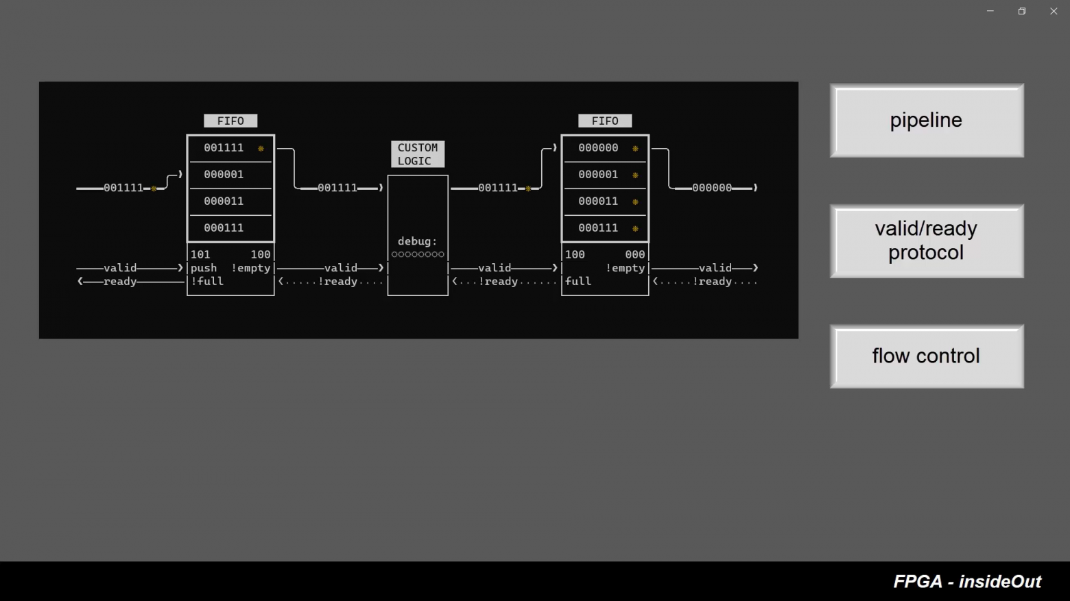
Exploring VALID/READY protocol, pipelines and experimenting with flow control using an HDL training tool
Ссылка на русскую версию / link to Russian version
Understanding valid/ready protocol is extremely important for every microarchitect.
Valid/ready is one of the main protocols used to organise flow-control inside a logic block as well as on inter-block (SoC) level.
In the last lesson, we explored FIFO buffer using hdlgadgets - human-in-the-loop HDL training tool.
This time we will take two FIFO buffers (which form a pipeline with valid/ready handshakes) and will experiment with it by changing flow-control logic of the pipeline.
We will show that valid/ready is not only a mechanism for transferring data from one FIFO queue to another, but also a method for organizing various kinds of logical functionality between queues.
If you have not worked with valid/ready protocol before, you will be surprised how easy it is to achieve desired functionality of the design by simply writing couple of lines of Verilog code in the handshaking logic block between two FIFOs.
Exploring FIFO principles using an HDL training tool
Ссылка на русскую версию / link to Russian version
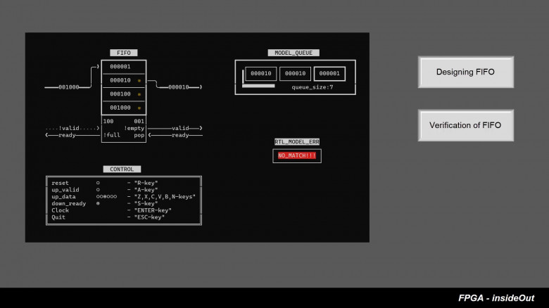
FIFO is a key concept in hardware design. Understanding of FIFO is necessary for understanding the valid/ready protocol, which in turn is necessary for organisation of flow-control within a design.
Unfortunately, there are very few books on this topic, and to be fair, microarchitectural concepts are quite difficult to master from books, since understanding of these concepts are coming with practice. In other words it is more about developing hardware intuition.
The idea of the HDL training tool is that it can help develop a hardware intuition, providing the opportunity to explore ready-made scenarios in a step-by-step interactive way. The tool also provides detailed visualization of a simulated scenario.
Since the tool is a front-end for the HDL simulator, the real, synthesized SystemVerilog is executed on the simulator itself, which can be viewed and even modified.
So, the video of exploring FIFO on the training tool is here:
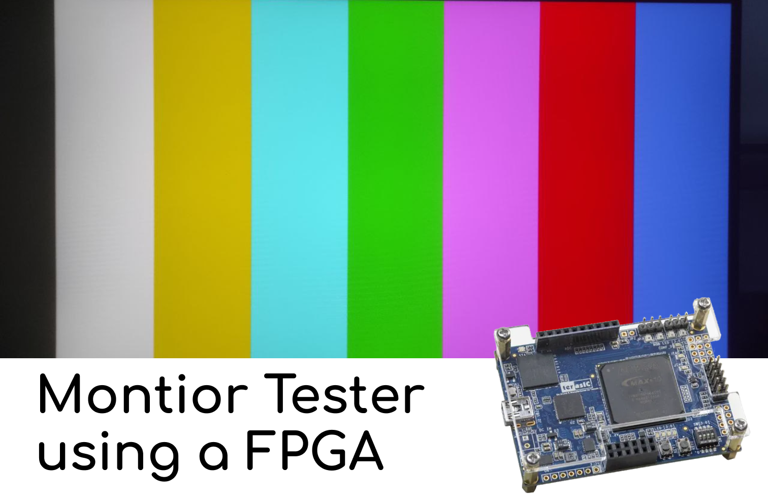
Testing a Monitor using DE10-Lite
In order not to buy a defective monitor, it is highly recommended to check it before buying. DE10-Lite is great for this because of a compact size and the presence of a VGA connector.
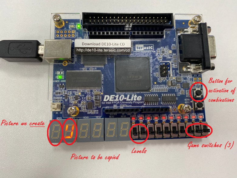
MemGame
We are the first year students studying Computer Science in Innopolis University and we would like to share our experience in developing a Verilog program to create the greatest Memory Game (MemGame) that has ever existed on the FPGA board.
In this article, we decided to create a game for extending human memory. You will read the background theory and the incredible story of creation.
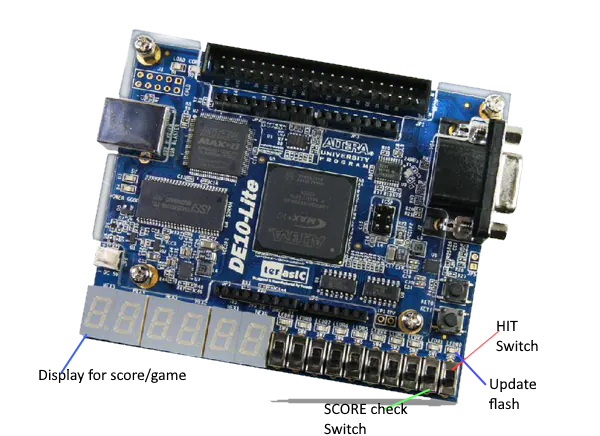
Clicker game by using FPGA and Verilog
Games can give positive emotions and provide relaxation to a person. However, the main purpose of my project is to get a better understanding of the Verilog language. In addition, coding a game into FPGA will help to define the bounds of this programming language.
“FPGA InsideOut” – animation about CRC and parallel CRC calculation
Ссылка на русскую версию / link to Russian version
FPGA InsideOut is an attempt to make a set of educational FPGA videos presented in the “human-in-the-loop” style. In these videos we will not only show how we are interfacing with an actual FPGA board but will also provide synchronous real-time visualisation of FPGA's internal logic.
For our first video we have picked a CRC circuit (cycle redundancy check) which is based on a linear feedback shift register. This circuit goes through several transformations during the course of the video. Intrigued? - let’s watch the video.
Music box on Verilog HDL for Cyclone IV E
Demid Efremov and Ivan Kornienko.
Music box on Verilog HDL for Cyclone IV.
The Dino game from Google Chrome using FPGA
Many people are familiar with the situation when there is no Internet, and a small dinosaur appears on the Google Chrome screen. Today we will tell you how to implement this game on the Cyclone IV FPGA board.
We are Yegor Blinov, Egor Kuziakov, and Inga Ezhova - the first-year students of Innopolis University. In our program, there was a course "Computer Architecture", where we had labs with FPGA boards Cyclone IV and MAX10. We were inspired by this equipment and decided to implement the project on one of the boards.
High-level pipelining in TL-Verilog, RISC-V from Imagination, formal tools and open-source EDA on ChipEXPO in Moscow
This year ChipEXPO conference in Moscow invited several Western speakers to present in English the emerging technologies in high-level HDLs, formal verification, open-source EDA and using industrual RISC-V cores for education. You can join these presentations on September 14-16 for free using this link (you may need to use google translate from Russian to go through the registration) https://eventswallet.com/en/events/282/
The whole program is here
The English-speaking presentations and tutorials include:
System-on-Chip bus: AXI4 simplified and explained
Protocol AXI4 was developed for High-bandwidth and low latency applications. It is designed to allow communication between master and slave devices. Master is typically a DMA or CPU and slaves are DRAM controllers, or other specific protocol controllers: UART, SPI, and others. Sometimes one component can implement multiple instances of this protocol. Usually, a prefix is used to differentiate between multiple AXI4 interfaces.
For example, Ethernet MAC can integrate DMA and slave interface used to command MAC. MAC can accept commands on the slave interface that contain data about the location of the next ethernet packet and MAC can start fetching this packet using the separate master interface instance.
This article was motivated by common design mistakes AXI4 designers make when they are designing their Digital IP. (Looking at you Xilinx)
Authors' contribution
YuriPanchul 2770.5megalloid 922.0KeisN13 603.5nckma 488.0hukenovs 429.0Armleo 421.3ishevchuk 419.0BarsMonster 281.0EasyLy 274.0ClusterM 246.0