
Хабр Курсы для всех
РЕКЛАМА
Практикум, Хекслет, SkyPro, авторские курсы — собрали всех и попросили скидки. Осталось выбрать!
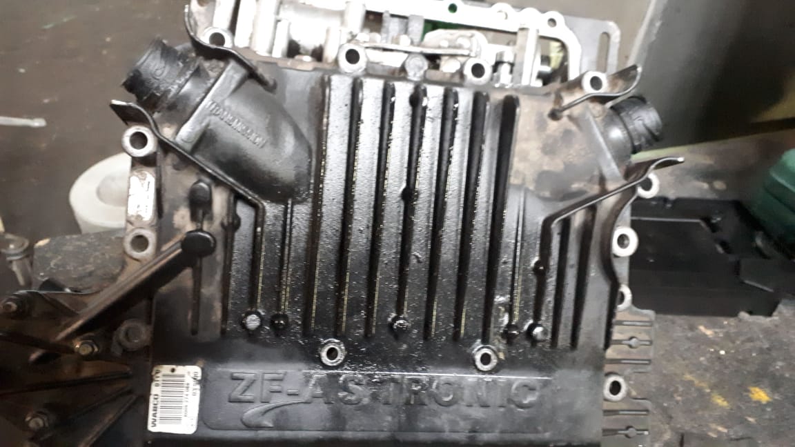
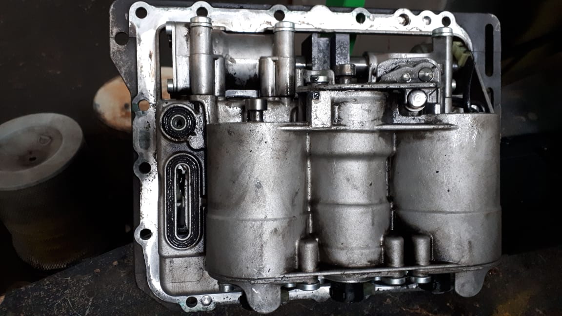
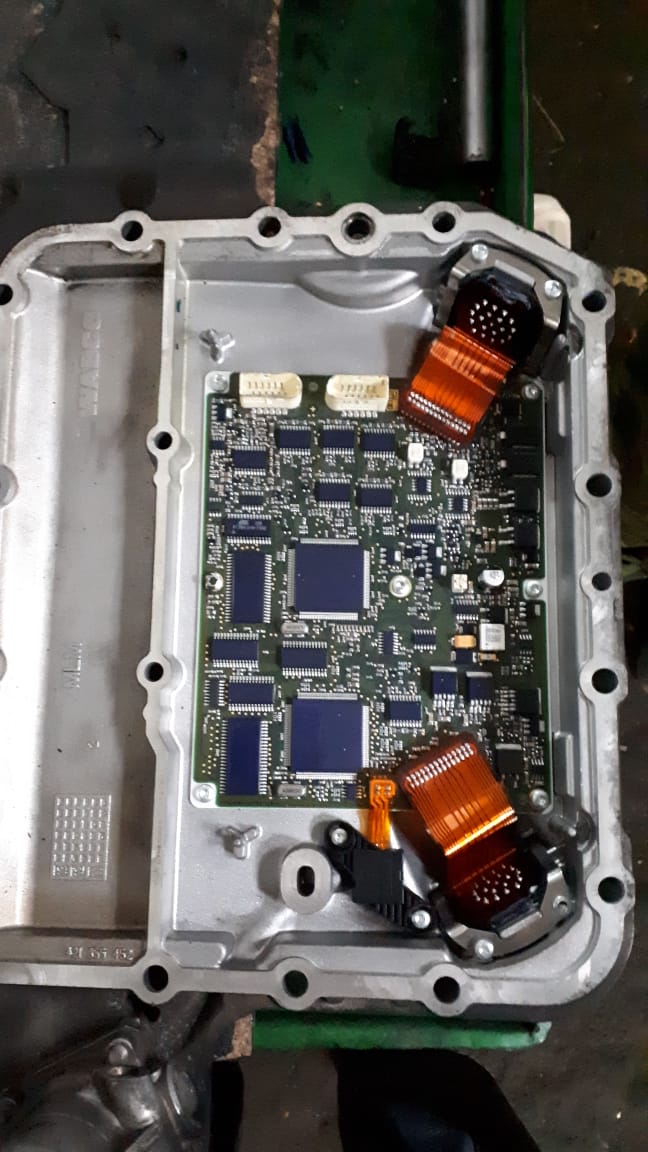
Алюминий? Очень странно, с его-то адским КТЛР. Разве что для силовых плат это сильно оправданно (мы делали платы для УФ-осветителей на алюминии — отличный теплоотвод и несущая конструкция в одном флаконе), но не для всех подряд. Корпус с шариковыми выводами на алюминии — это же просто песня!
Насчёт лака верно, хотя от термоциклов это спасает мало, как и от тряски. Но насчёт tssop — люто несогласен. Огромное количество MCU/CPU для автомобилей вообще не имеет не-bga исполнения.
… deposition of solder bumps on i/o pads...
… A plurality of solder balls is included, each of which has a polymeric core surrounded by a metallic shell that in turn is surrounded by a layer of solder material. Further, each solder ball is positioned in contact with a corresponding contact pad of the package. An intertwined intermetallic fusion layer is formed through the fusion between material components of the contact pads and the solder material, via heat treatment. The intermetallic fusion extends between and from an outer surface of the metallic shell of each solder to an outer surface of a corresponding contact pad to form a high strength intermetallic solder joint therebetween.
Typical micro SMD packages contain bump counts ranging from a four (4) (2×2 array outline) bump count to a thirty (30) bump count (5×6 array outline). At these smaller bump counts, the active side of the array are mounted to a Printed Circuit Board (PCB) in a manner similar to a typical Ball Grid Array (BGA) mount, via conventional solder joints. These packages, given their dense array of I/O contacts, are limited to about thirty (30) bumps due to the solder joint fatigue life. In general, the outer I/O contacts of a package, when mounted to a circuit board, are subjected to greater loading stress than those contacts that are central to the package due to greater DNP (Distance from Neutral Point). Such joint stress, for instance, may be experienced during thermo-cycling and/or during a drop testing. Due in part to the geometry and position of these outermost contact posts relative to those contacts centrally located, any central loads are magnified significantly at the perimeter of the package. Accordingly, contact failure at such outermost contact interfaces is more prevalent.
More recently, Micro SMDxt packages have been developed that have significantly larger bump counts than the array of contacts for a standard SMD package (typically up to a 5×6 array, or 30 bump count). These Micro SMDxt packages 25, as shown in FIG. 1, generally range from thirty-six (36) bumps (a 6×6 array outline) to 100 bumps (a 10×10 outline).
To enable solder mounting of these larger array Micro SMDxt packages, each solder joint incorporates a solder ball consisting of a polymeric core with a copper shell followed by an outer solder layer. Applying a single industry standard reflow process, a significantly higher strength joint can be created due to the flexibility of the polymeric core. Hence, a significantly longer fatigue life can be achieved than a conventional solder joint. Typical of such polymeric core solder balls are those commercially available by Sekisui Corporation of Japan.
However, proliferation of this package family beyond 100 bumps (10×10 array outline) is limited by the solder joint fatigue life. While the polymeric core allows a longer fatigue life than convention solder joints, it still reaches its limit in terms of fatigue life and life under drop/impact conditions.
екоторые примеры испытаний, в том числе в зависимости от параметров миссий NASA, приводятся в статьях западных коллег [1, 4, 5]. На этом вопрос «пластика» в океане космосе считаю открытым закрытым.


SamsPcbGuide, часть 12: Технологии — корпуса BGA-типа, пластик и космос II