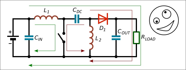
Knowing parameters of small-signal control-to-output transfer functions makes it easier for engineers to design compensation networks of DC/DC converters. The equations for SEPIC can be found in different works and Application Notes, but there are differences. A work has been done to solve this problem.
Simplified design equations for SEPIC with Current Mode control (CM) in Continuous Conduction Mode (CCM) suitable for practical design of compensation networks are shown.
Known equations
It looks like that the compensation design equations for SEPIC in Application Notes are based on the equations taken from “A tutorial for small signal models in the SEPIC power stage” by Joel Steenis, National Semiconductor, [2]. There are also less known works: “Analysis of the Sepic Converter” by Dr. Vatché Vorpérian, [1] and TI, AN-1990, “Compensation for Current Mode Control SEPIC Converters”, [3].
Mistakes are seen in [1] and [2]. See, for example, the A2, A3, A4 definitions and later ωz in [2], or the a3 and DC gain definitions in [1]. Equations in [3] are huge and it is not clear how to use them. There are also works on the researchgate web site.
SEPIC CM CCM small-signal equations
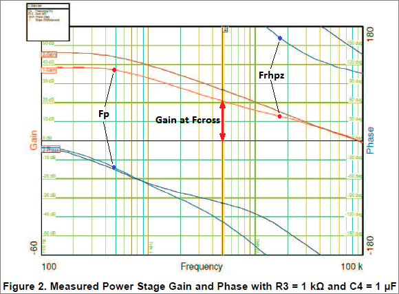
The figure below, taken from TI’s AN-1990 [3], shows what the small-signal control-to-output function might look like.

Thanks to Christophe Basso, the small-signal control-to-output transfer function for SEPIC CM CCM was obtained. The full equation is huge, thus only simplified equations are shown for key parameters.
The small signal control-to-output transfer function of SEPIC CM CCM may be written as the following:
           1 + n1 × s + n2 × s^2 + n3 × s^3 + ...
H(s) = Adc ——————————————————————————————————————
           1 + d1 × s + d2 × s^2 + d3 × s^3 + ...
The order depends on parameters taken into account. The nominator is at least 4th order and denominator is at least 5th order.
It can be rewritten in more useful form as in [9]:
           (1 − s / ωrhpz) (1 + s / ωesr)
H(s) ≈ Adc —————————————————————————————— He(s)
                    (1 + s / wp)
Where:
Adc – the DC gain, times;
ωp – the main pole frequency, rad;
ωrhpz – the right-half plane zero (RHPZ) frequency, rad;
ωesr – the zero caused by the output capacitance and its equivalent series resistance, rad;
He(s) – models the inductor current sampling effect as well as the slope compensation effect;
The magnitude at the desired crossover frequency is:
             √{F² / Frhpz² + 1} × √{F² / Fesr² + 1}
|H(F)| ≈ Adc ——————————————————————————————————————
                       √{F² / Fp² + 1}
All the frequencies here and later are in Hz. He(s) is ignored because it is well above the crossover frequency. If the Fesr frequency is much higher than the crossover frequency, this member may also be ignored.
There is also a pair of double pole and zero creating a “glitch” due to resonances caused by the coupling capacitor and inductors. Since it looks like a “glitch”, there is no sense to use it in the equation for magnitude at the crossover frequency.
The main resonance frequency, a first order pole, is:
       (1 + D) × Iout       (1 + D)
Fp ≈ ————————————————— = ——————————————
     2 π × Cout × Vout   2 π × Cout × R
The RHPZ frequency is:
                        (1 − D)² × R
Frhpz ≈ —————————————————————————————————————————————
        2 π × D × [(1 − D) × K × √{L1 × L2} + D × L1]
The DC gain is:
      Vout × Gmps × (1 − D)        Vout × (1 − D)         R × (1 − D)
Adc ≈ ————————————————————— = ——————————————————————— = ————————————————
         Iout × (1 + D)       Iout × Rsense × (1 + D)   Rsense × (1 + D)
The “glitch” frequency is:
                                1
Fglitch ≈ —————————————————————————————————————————————
          2 π × √{Cdc × (L1 + L2 − 2 × K × √{L1 × L2})}
Where:
Vout – the output voltage, V;
Iout – the load current, A;
R – the load, Vout / Iout, Ohm;
Cout – the output capacitance, F;
Rsense – the current sense resistance, Ohm;
L1 – the first, input inductance, H;
L2 – the second, output inductance, H;
K – the coupling coefficient of the inductors;
Cdc – the coupling capacitance, F;
D – the duty cycle.
The equation shows that the “glitch” frequency can be low when uncoupled inductors are used and should be taken into account. With tightly coupled inductors there is no glitch which is consistent with measurements [8].
Now a compensation network can be designed.
Compute the Fp, Frhpz, Fesr, Fglitch;
Choose a crossover frequency Fcross, between the Fp and the minimum of Frhpz and Fglitch;
Compute the magnitude at the crossover frequency and set the compensation network gain to the 1/gain value;
Set the zero of the compensation network below the Fp and the pole somewhere around the Frhpz or Fesr;
Example
Let’s compute the values to design a compensation network and compare the results with data from [6].
The requirements: Vin = 9…24 V, Vout = 12 V, Iout = 0.75 A, Fsw = 750 kHz.

In the circuit: Cout = 32 uF, L1 = L2 = 47 uH with 0.99 coupling, Rsense = 40 mOhm from the TPS61175 datasheet.
Calculate the values for the worst case at the minimum input voltage and maximum load.
The duty cycle at the minimum input voltage is: D = 0.58.
The load resistance is:
    Vout    12 V
R = ———— = —————— = 16 Ohm
    Iout   0.75 A
The DC gain is:
         R × (1 − D)      16 Ohm × (1 − 0.58)
Adc ≈ ———————————————— ≈ ————————————————————— ≈ 106 ≈ 40.5 dB
      Rsense × (1 + D)   0.04 Ohm × (1 + 0.58)
The main pole frequency is:
         (1 + D)           (1 + 0.58)
Fp ≈ —————————————— ≈ ——————————————————— ≈ 480 Hz
     2 π × Cout × R   2 π × 33uF × 16 Ohm
Since Resr is unknown in the circuit, let it be 20 mOhm, then the ESR zero frequency is:
               1                     1
Fesr ≈ ————————————————— ≈ ————————————————————— ≈ 240 kHz
       2 π × Cout × Resr   2 π × 33uF × 0.02 Ohm
The RHPZ frequency is:
                       (1 − D)² × R
Frhpz ≈ —————————————————————————————————————————————
        2 π × D × [(1 − D) × K × √{L1 × L2} + D × L1]

                      (1 − 0.58)² × 16 Ohm
≈ ——————————————————————————————————————————————————————————————— ≈ 16.5 kHz
  2 π × 0.58 × [(1 − 0.58) × 0.99 × √{47uH × 47uH} + 0.58 × 47uH]
The glitch frequency is:
                                1
Fglitch ≈ —————————————————————————————————————————————
          2 π × √{Cdc × (L1 + L2 − 2 × K × √{L1 × L2})}

                             1
≈ ———————————————————————————————————————————————————————— ≈ 164 kHz
  2 π × √{1uF × (47uH + 47uH − 2 × 0.99 × √{47uH × 47uH})}
A crossover frequency must be in several times lower than the minimum of the RHPZ and glitch frequency. The chosen crossover frequency in [6] is 5 kHz.
The ESR zero frequency is ignored because it is too high, so the gain at 5 kHz is:
             √{F² / Frhpz² + 1}       √{5kHz² / 16.5kHz² + 1}
|H(F)| ≈ Adc —————————————————— ≈ 106 ——————————————————————— ≈ 10.6 ≈ 20.5 dB
              √{F² / Fp² + 1}          √{5kHz² / 480Hz² + 1}
Now we can compare the computed values with the measurements in Figure 2 in [6].

A Type II compensation network can be used with any schematic.
The middle frequency gain around 5 kHz should be set around 1/10.6 or −20.5 dB;
The zero frequency should be around 500 Hz;
The pole frequency should be somewhere at a frequency higher than 15 kHz.
The circuit uses Type IIa compensation with built-in transconductance amplifier without explicit pole frequency. Its parameters are: the zero frequency is 1 kHz to compensate the main pole, the gain at 5 kHz is −23 dB.
The figure below shows the result. Since the gain of the compensation network is lower than −20 dB, the crossover frequency is not 5 kHz, but about 4 kHz.

And let’s look how a circuit with the same input parameters and its small-signal control-to-output transfer function would look in a design tool.

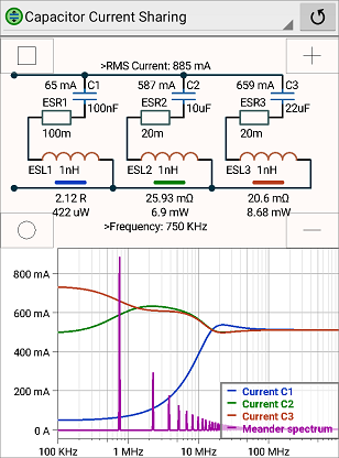
Pay attention that C6 1uF in the original circuit has too low capacitance. The C6 capacitance should be increased to reduce circulating currents, see [10] and [11].


Conclusion
Equations are able to simplify design of compensation networks.
Equations of small-signal control-to-output transfer functions of DC/DC converters can be found, for example, in [9], [12], [13], [14]. But keep in mind that the equations are simplified and the curves are different from real ones, especially in high frequency range.
Measurements for SEPIC in different modes can be found here: “Practical control measurements for the Sepic converter”, [8]. Unfortunately, some details are missed there.
Christophe Basso published his new book “Transfer Functions of Switching Converters” recently about small-signal modeling, [14]. You can also find a lot of other useful information on his site [12].
Such tools like “Power Stage Designer Tool”, “LTpowerCAD”, “Circuit Calculator” are intended to simplify work for engineers and offer equation-based design.
References
Dr. Vatché Vorpérian, “Analysis of the Sepic Converter”. Ridley Engineering. Power Systems Design Europe, November 2006. Link.
Joel Steenis, National Semiconductor, “A tutorial for small signal models in the SEPIC power stage”. Link.
Texas Instruments, AN-1990 Compensation for Current Mode Control SEPIC Converters. Link.
Texas Instruments, AN-1484, “Designing A SEPIC Converter”. Link.
Texas Instruments, TPS61175 datasheet. Link.
Texas Instruments, SLVA384, “Designing a Split-Rail SEPIC With the TPS61175”. Link.
Texas Instruments, Markus Zehendner, Matthias Ulmann, “Power Stage Topology Reference Guide”. Link.
Ridley Engineering site. Link.
Power Stage Designer User Guide, Chapter 11. Link.
Power Tip 32: Beware of circulating currents in a SEPIC coupled-inductor – Part 1. Link.
Power Tip 33: Beware of circulating currents in a SEPIC coupled-inductor – Part 2. Link.
Christophe Basso, personal site. Link.
Christophe Basso, “Switch-Mode Power Supplies, Second Edition: SPICE Simulations and Practical Designs”, 2nd Edition. Link.
Christophe Basso, “Transfer Functions of Switching Converters”. Stairway Press. Link.
Power Stage Designer Tool. Link.
LTpowerCAD. Link.
"Circuit Calculator", an electronics circuit design tool for Android. Link.