Introduction

Protocol AXI4 was developed for High-bandwidth and low latency applications. It is designed to allow communication between master and slave devices. Master is typically a DMA or CPU and slaves are DRAM controllers, or other specific protocol controllers: UART, SPI, and others. Sometimes one component can implement multiple instances of this protocol. Usually, a prefix is used to differentiate between multiple AXI4 interfaces.
For example, Ethernet MAC can integrate DMA and slave interface used to command MAC. MAC can accept commands on the slave interface that contain data about the location of the next ethernet packet and MAC can start fetching this packet using the separate master interface instance.
This article was motivated by common design mistakes AXI4 designers make when they are designing their Digital IP. (Looking at you Xilinx)
Channels
Channels are carriers of channel transactions. AXI4 implements 5 channels:
Read Address: AR, channel from master to slave
Read data: R, channel from slave to master
Write Address: AW, channel from master to slave
Write data: W, channel from master to slave
Write response: B, channel from slave to master
Each channel follows channel protocol rules, which are described in the next section. Read-only and Write-only variations are possible. This is done by implementing only channels required by a specific device. AXI Specification also defines AXI4-Lite protocol which imposes more strict rules to transactions generated by the master. Any AXI4 slave can be connected to AXI4-Lite master, however, only AXI4 masters following AXI4-Lite rules can be connected to AXI4-Lite Slaves.
Channel Rules
Each channel consists of VALID/READY handshake signals and channel payload signals. Channels have their direction, which matches the direction of the signal VALID. READY has opposite direction of VALID signal.
For each channel, it is required for VALID to be asserted to signal the start of the channel transaction. The receiver side asserts the READY signal to let the channel master know that the channel transaction was accepted and the next channel transaction can be started. One channel transaction is defined as an assertion of VALID signal followed by the asserted READY signal for one cycle. Channel payload signals should not change while the transaction is active and VALID signal should not depend on value of READY signal (looking at you Xilinx). VALID can't be deasserted until READY is asserted (again looking at you Xilinx).

Advantages of dividing groups of signals into channels is the simplification of Clock, Power and Reset domain crossing, register slicing ("period slicing"). This will be further elaborated below. It also further clarifies signal relations, because different channels have different valid signals and prefixes, it is hard to accidentally misunderstand which signals are valid at which stage.
AXI4 signals
AXI4 requires for interface to implement ACLK which carries clock signal and requires that signals in each channel be valid on the rising edge of this clock signal. It is also required to implement ARESETn which is when low, signals reset. While reset is asserted and one cycle after reset it is required to drive all channel valid/ready signals low.
Following signals are implemented for the AW/AR channels going from master to slave:
AW channel signal name | AR channel signal name | Description |
AWVALID | ARVALID | Handshake signals |
AWREADY | AWVALID | |
AWID | ARID | Carries identifier. More about this is explained in section: xID signals explained |
AWADDR | ARADDR | Transaction address generation and calculation-related signals. Explained in address generation and calculation section. |
AWLEN | ARLEN | |
AWSIZE | ARSIZE | |
AWBURST | ARBURST | |
AWPROT | ARPROT | |
AWLOCK | ARLOCK | Explained in atomic operations |
AWCACHE | ARCACHE | As explained at the end of this section. |
Following signals are implemented for the W channel going from master to slave:
Channel signal name | Description |
WVALID | Handshake signals |
WREADY | |
WDATA | Write data |
WSTRB | Write strobe (active-high) |
WLAST | Signals last channel transaction for this transaction. |
Following signals are implemented for the B channel going from slave to master:
Channel signal name | Description |
BVALID | Handshake signals |
BREADY | |
BID | Carries identifier. More about this is explained in section: xID signals explained |
BRESP | Response explained in "Writes explained" |
Following signals are implemented for the R channel from slave to master:
Channel signal name | Description |
RVALID | Handshake signals |
RREADY | |
RID | Carries identifier. More about this is explained in section: xID signals explained |
RDATA | Response Data, bus aligned |
RRESP | Response, explained in "Reads explained" |
RLAST | Signals last channel transaction for this transaction. |
Example transactions with expanded signals are presented below.
Read requests explained
AXI4 read requests happen on channels AR and R. AR channel is used by the master to send read requests to slave. Master first sets the AR channel signals like ARADDR, ARSIZE, ARBURST ARLEN and many more signals. Then ARVALID is asserted signaling that new transaction is started.
Slave then asserts ARREADY, letting master know that the transaction has been accepted and response will be returned on R channel.
Slave after the cycle it accepts AR channel transaction sets R channel signals like RRESP, RDATA and RID.

For one AR channel transaction, multiple responses may follow. Each R channel payload is called "beat". Multiple beats with one last beat asserting xLAST signal is called a burst. A single AR request with a single burst on the R channel is called AXI read transaction.

AR channel signals are explained in other sections. R signals are the following: RRESP, RDATA, RLAST, RID and obviously, handshake signals. ARLEN contains the number of beats minus one. Slave uses this information to generate response data beats matching ARLEN + 1. Each beat RID signal should contain the same value as ARID when the transaction was started. Multiple transactions can be started to compensate for interconnect and slave delays. It is required for slaves to respond in the same order as was requested only if these transactions have the same IDs.
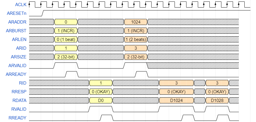
Let's take a look at some transactions, see waveforms below. In RDATA Dy shows that for transaction data from address y was returned. The first transaction in light yellow is one beat long burst. The second is an INCR two-beat burst.
In the waveform below is WRAP four-beat burst.

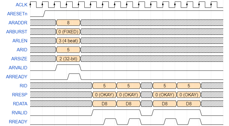
In this waveform is a FIXED four-beat burst.
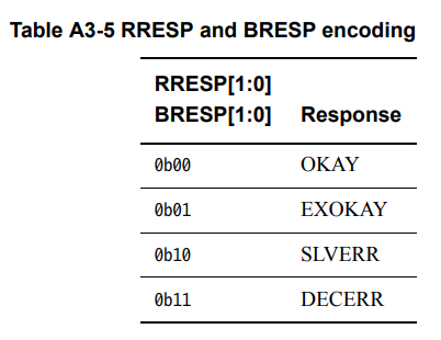
RRESP/BRESP has the following values. EXOKAY is explained in the atomic access section.
Slaves can choose to accept write or read first or both, however after write response has been transferred on B bus memory slave devices have to respond with updated value for each read.
Interconnect and crossbar relies on xLAST signal to differentiate between multiple signals, and as explained in "xID signals explained" interconnect extends ID bits to contain information about requester, and when data is returned same ID bits are used to make a decision about which master response has to be directed to.
One of the common mistakes of designers is assuming that the R channel RRESP signal stays the same between multiple beats in the same burst. It's wrong each beat may contain a different response.
The second most common mistake is assuming that ARREADY is not required to be asserted before asserting RVALID. This is not the case as explained in section "Relationships between the channels" in the AXI4 specification.
The third most common mistake is to assume that if multiple AR transactions are started, they are going to complete in the same order as requested if they have different IDs. This is not the case as explained in the section "Relationships between the channels". Slaves are required to keep multiple transactions with the same ID in the same order as requested, but this requirement is not valid for transactions with different IDs.
Write requests explained
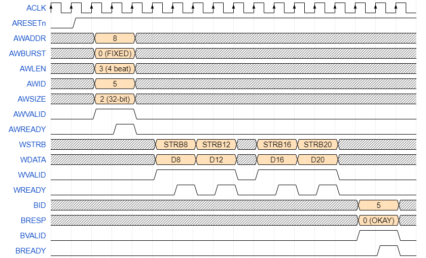
Write transactions are started by request on the AW channel. Master sets AW signals like AWADDR, AWSIZE, AWLEN, AWBURST, etc. Then master raises AWVALID.
At the same time master also sets data on W channel, like WSTRB, WDATA, WLAST. Master is not allowed to wait for AW channel request to be accepted before asserting WVALID. Violating this may cause deadlocks.
Each bit in WSTRB corresponds to a single 8 bit byte in WDATA. If WSTRB is asserted then the corresponding byte in WDATA is written, otherwise it's ignored. WSTRB is required to correspond with AWSIZE and should be aligned with AWADDR.
Bit in WSTRB | 3 | 2 | 1 | 0 |
Corresponding bits in WDATA | [31:24] | [23:16] | [15:8] | [7:0] |
When slave is ready it raises AWREADY to signal that it's done with data on AW channel. Slave also raises WREADY signaling master that write data is accepted. Then WVALID/WREADY steps are repeated for each beat in that transaction. On last beat master asserts WLAST.
After last WVALID/WREADY with WLAST asserted slave sets signals on B channel like: BID, BRESP and then raises BVALID to signal to master that response to write is done. Master when ready asserts BREADY, signaling completion of the transaction.

One of the common mistakes is to assume that the master is allowed to wait for AW to be accepted before putting W channel data. This assumption is wrong and may create a deadlock (looking at you Xilinx). For optimal performance, it is recommended to put AW channel data and W channel data as early as possible.
After AW and W channel the last beat is accepted, the slave is allowed to assert the BVALID signaling response on the B channel. B channel contains a BID signal which should match the same value as in the AW channel request. BRESP matches its encoding with RRESP.
Masters have to put W channel data in the same order as AW channel's data. Mixing orders between multiple transactions on AW and W channels is not allowed.
Let's take a look at some examples.
")
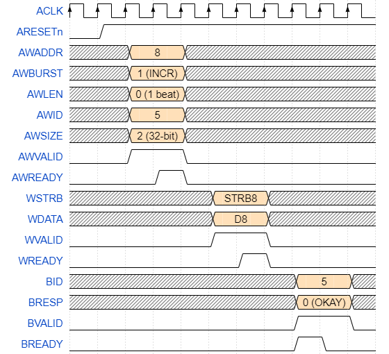
Now let's take a look at another one beat INCR burst.
Now let's take a look at 4 beat INCR burst.
Signal widths
There are parameters defining the widths of some of the signals: Data width, Address width, and ID width.
I usually use fixed data width and configurable address/id width. Sometimes address bits are required to be some number of bits, by slave implementation.
Data width conversation is done by data bus width converters and AXI4 implements signals that are used to facilitate this form of conversation. One of these signals is AxSIZE, however, implementation has to follow rules for AxCACHE bits.
Address width conversation is usually done depending on the exact implementation. Most implementations just append zeros to widen and throw away unnecessary bits to narrow address width. Throwing away address bits is highly not recommended because it may result in some locations being unavailable. RISC-V-based CPUs who use AXI4 for their bus use signed number extension, because that's what specification RISC-V requires, however, this is usually done by CPU implementation itself, instead of interconnect/crossbar.
ID width down conversation is unreasonable but easy to implement by mapping multiple IDs to the same ID and then remembering in which order for that ID request has been sent. When the response arrives we unmap narrow ID to wide ID because we know that for the same ID transaction order is preserved.
ID up conversation is simply done by left appending zeros. Usually, interconnect and crossbar extend ID width to include information about transaction source. When the response arrives, this ID is then used to redirect the response to the master that initiated the transaction.
ARCACHE/AWCACHE signals
ARCACHE and AWCACHE signals are used to give cache/crossbar and interconnect a suggestion about the requirements for the transaction: cache allocation, bufferability, modifiability policy. All valid values and explanations of specific bits that can be found in the AXI4 specification fall outside the scope of this article.
Address and burst logic
AXI4 implements burst transactions to increase performance and implements multiple active transactions to improve performance in high latency systems. Both read and write transactions are initiated on AR/AW channels accordingly. AR and AW channels contain four signals used in address generation and bursting logic: AxADDR, AxSIZE, AxLEN, AxBURST.
AxADDR contains starting address, however, it might not be bus size aligned for some burst types. All addresses are byte-aligned values.
AXI4 defines the following: The single beat is data on W channel or R channel from when VALID is asserted to when READY is asserted. Multiple beats can be transitioned on the W/R bus, the count of these beats is defined by AxLEN value plus one. The last beat always asserts xLAST signal, to signal to interconnect that single burst was done. Single burst is defined as all the beats from the first one to the last beat with xLAST signal asserted. One transaction contains one address beat and AxLEN + 1 data beats. For writes, this also includes one beat at B channel, which contains RESP and ID signals of the transaction.
, T2 (arlen=3) read transactions and T3 (awlen=1), T4 (awlen=3) write transactions.")
AxSIZE signal contains log2 value of the count of bytes that are going to be transferred in a single beat. AxSIZE can be as high as the maximum size of the data bus. AxSIZE is not mandatory for master and if not implemented then value matching data bus width is used. Slaves have to implement this signal. AxSIZE does not change the number of beats in a single transaction but instead specifies a single beat's width.
AxSIZE | Bytes in transfer |
0 | 1 |
1 | 2 |
2 | 4 |
3 | 8 |
... | ... |
7 | 128 |
AxLEN specifies the number of beats in a single transaction minus one. For example, value of zero means that there is one single beat. This signal is not mandatory for masters and if not implemented by the master, then a value of 0 (single beat) is assigned to the slave's input.
AxBURST controls internal address generation and allows to choose between FIXED - same address for all beats, INCR - each beat address is incremented by 1 << AxSIZE and WRAP - each beat address is incremented by 1 << AxSIZE but addresses are wrapped, in other words first beat starts at the address specified by AxADDR and is incremented by 1 << AxSIZE, however when bits that match AxLEN's value rollover they cause the next addresss' same bits to start from 0. For WRAP bursts it is required for AxLEN to be any value of: 1, 3, 7, 15. For all bursts, addresses need to be aligned according to AxSIZE.
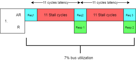
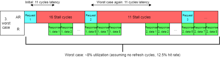
Before we move on, let's discuss why we even need such complex pipelined and burst interfaces. Let's discuss one very common case: We have SDRAM controller that accepts address data and then 11 cycles later provides response data that was read from memory.
1) Most simple implementation would just accept one address data and then provide singular 8 byte data from memory 11 cycles later. This means that best case scenario we have one data cycle in 13 cycles or 7% efficiency and 11 cycles latency.
2) Now let's optimize it. Instead of only reading one cycle of data, instead, we request a section of data from DRAM memory and then cache it. We need 8 bytes but it is extremely likely that we will need adjacent data (for example, because it's a continuous stream of instructions).
Let's say instead of requesting 8 bytes for each transaction we request 64 bytes (8 words) starting from byte 0 in a cache line.
Let's assume a 50% hit rate. Easy to calculate that in 20 cycles we read 64 bytes and used 32 bytes, this means we achieved 4 data words in 20 cycles efficiency or about 20% and 20 cycle latency.
For 12.5% hit rate we get 5% bus utilization and for 100%, bus utilization reaches 40%.

3) Now let's imagine that our DRAM can accept address in 3-11 cycles (yes 0 wait cycles before providing next data beats) before it provides data. This is because address in DRAMs uses a separate bus making it possible to start the next transaction before the last one completes.

Depending on locality it may be required to issue multiple operations on the address bus (open column and only then open row), reducing performance and increasing latency. Not hard to calculate that we would achieve about 23%-100% efficiency (assuming no refresh cycles) depending on how local requests were and 11-20 cycle latency depending on which data is required by request (assuming all operations need to be done) or up to 3-12 cycles latency if an only open row operation is required.

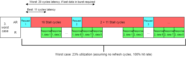
4) By implementing both INCR bursting and pipelining we utilized 100% of our bus, but we still have 3-20 cycles delay between our request and data, because we start fetching data from byte 0 of the cache line.
Depending on if we need the first or the last word in a cache line the latency varies between 11-20 cycles. The solution is using WRAP bursts instead of INCR bursts. This way, the data word which is required, will be fetched first allowing us to still get 100% bus utilization AND reduce latency to the same level as initial implementation.
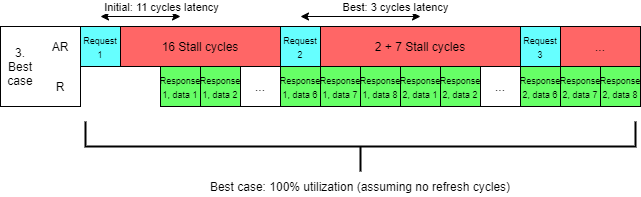
All current SoCs and all DRAM implement WRAP bursts for cached access AND pipelined memory access, because it's simply inefficient to do it any other way.
AXI4 requires specific values for AxLEN signal in WRAP burst requests because SDRAM memory uses a specific fixed set of values for burst length.

In comparison FIXED bursts allow DMAs and CPUs that utilize FIXED bursts to read/write multiple data samples to the same location. This is useful for example if you have audio samples that are being read from memory and are streamed to the audio controller, which accepts data in a single address location.

Mapping of AxBURST values and burst types are presented below. For bursts where AxLEN is set to zero, it is recommended to set AxBURST to INCR.
AxBURST[1:0] | Burst type |
0b00 | FIXED |
0b01 | INCR |
0b10 | WRAP |
I implement burst logic in slave as follows (given example for Verilog, not compiled, may be bugged, use at your own risk):
increment = (1 << (size)); // 8 bits wide
// Size = 0, 1 byte, 1 increment
// Size = 1, 2 byte, 2 increment
// Size = 2, 4 byte, 4 increment
// etc

// Wrap mask. Bit mask showing
wrap_mask = (len << size) | (increment - 1);
// Width matches address width,
// assumed that address can fit full burst
// Examples:
// size = 3'b010,
// len = 8'b0, 1 cycle,   wrap mask = 11
// len = 8'b1, 2 cycles,  wrap mask = 111
// len = 8'b11, 4 cycles,  wrap mask = 1111
// len = 8'b111, 8 cycles,  wrap mask = 11111

// addr_nxt is signal for next address
// addr is current addr
if(burst_type == `AXI_BURST_INCR)
    addr_nxt = (addr + increment) & ~(increment - 1);
    // make sure that all subsequent addresses are aligned to size
else if(burst_type == `AXI_BURST_WRAP)
    // make sure that wrap actually wraps around,
    // by throwing away unnecessary carry bits
    // no need to reset LSB bits because it is required for addr to be aligned
    addr_nxt = (addr & ~wrap_mask) | ((addr + increment) & wrap_mask);
else if(burst_type == `AXI_BURST_FIXED)
  	addr_nxt = addr; // Fixed address :D
As mentioned in the AXI4 specification bursts can't cross 4KB boundaries. My crossbar maps AXI4 slaves to 4KB aligned regions because it makes bursting across multiple slaves impossible.


For INCR bursts it is required for the address to be aligned according to the value of AxSIZE. This is done to allow the narrow bus to wide bus conversation. It is common to assume that address is aligned to bus width, which is wrong.
Another common mistake is: assuming endianness. AXI4 is specifically designed to be byte invariant. This is explained really well in the AXI4 specification itself and falls outside of the scope of this article.
ARPROT/AWPROT
Both AR and AW implement additional ARPROT/AWPROT, which contain three bits used by ARM processors to signal to slave current privilege level. Three bits are defined as following:
AxPROT bit | Value | Description |
0 | 0 | Unprivileged access |
1 | Privileged access | |
1 | 0 | Secure access |
1 | Non-secure access | |
2 | 0 | Data access |
1 | Instruction access |
If slave behaves differently depending on AxPROT bits, it can use these bits in address decode logic. Use cases for these bits include peripherals that are only visible in secure mode, or only in privileged mode. For example, Boot memory with a bootloader can be made invisible to supervisor-level software (kernel).
Transaction IDs and their usage
Each transaction on the AXI4 bus can have an ID. ID is supplied by the master at AW/AR channel and returned on R and B channels. Usually out of order CPUs use the ID to their own needs, like what register data will be written back or for signaling different threads in the same core. This allows the CPU to make multiple read or write requests while no data or response arrived.
Another use case is by crossbars. Crossbars extend ID bits by $clog2(number of masters). This allows the crossbar to know to which master to redirect response, then ID bits that were used for this purpose are stripped and a new ID is returned to requesting master that matches the ID of the original request.
 is appended to original transaction's ID (light blue) to then use the appended bits to identify master that started the transaction. Only original transaction's ID (light blue) is returned to master.")
Master's number (green) is appended to original transaction's ID (light blue) to then use the appended bits to identify master that started the transaction. Only original transaction's ID (light blue) is returned to master.
AXI4 defines that only transactions with the same IDs have to be in order, this means that the crossbar can take advantage of this by initiating multiple transactions from multiple masters, to minimize bus idle time and reduce performance hit done by latency.
Atomic operations explained
Let's imagine the following. We have a website that is used to vote for candidates for the presidency at the Banana Republic. Obviously, the website handles a lot of traffic, so we decided to handle multiple transactions in parallel.
When a request to vote comes the handler just increments the variable stored in the memory. However, multiple votes can come to different handlers each running on its own CPU. The problem may arise, where CPU0 reads current counts of votes. Then CPU1 reads current counts of votes. CPU0 increments and writes back a new count of votes, but CPU1 still uses stale value of votes, increments and writes back a different count of votes that does not include votes produced by CPU0.

One of the possible solutions is CAS operation or compare-and-swap. The first value is read and modification of the internal register is done (for example it's incremented). Then CAS operation is done and swap of internal register and memory location is done only if the value of the original read matches the value in memory, otherwise, the swap does not complete. This means that if the value has been modified by another CPU, then the CAS will fail, letting software know that increment did not succeed and to attempt it again.
CAS suffers from an ABA problem. ARM, MIPS, RISC-V, and other RISC CPUs propose different solutions to this problem: Load reserve/store conditional operations.
Load reserve tells memory to raise an internal flag for some amount of memory that includes the initial load operation's location. When any store is done to the same reserved location that flag is reset. When CPU attempts store conditional it fails because the reservation has been reset. CPU now retries to do the same operation by repeating the attempt. If the flag is still raised and the store-conditional operation has the same ID as the original load-reserve, the operation succeeds. It is allowed to fail this operation for any arbitrary reason.

Let's see why it is required for the ID of the original load-reserve. Let's imagine attacker CPU executes continuously store operation causing the exclusive monitor to remove reservation, so victim CPU will never successfully complete store-conditional causing deadlock for victim CPU.
The exclusive monitor mitigates this by implementing multiple locks that match at least number of CPUs, this way attacker CPU will only mess up its own reservations. This is done by requiring the initial ID number to match the ID of store-conditional and CPUs to use separate values for each thread. Usually, implementations implement multiple exclusive monitors, count of which matches count of all of the possible ID values.
However, stores still invalidate the exclusive monitor's lock if the same location as in the original load-reserve is overwritten. This is safe because if multiple threads share the same memory locations then the threads already trust each other.
Now let's take a look at what AXI4 implements to allow the implementation of load-reserve and store-conditional operations. First of all, it's an additional AxLOCK signal. When load operation is done with ARLOCK asserted it's called load-reserve operation. And store operation with AWLOCK asserted is called store-conditional.
Some slaves may not support exclusive access. To signal this to the CPU slaves can just ignore ARLOCK signal because for successful exclusive access separate response value is used: EXOKAY. If the slave does not implement the ARLOCK signal then load-reserve to any location will result in a response OKAY (which is different than EXOKAY) signaling to the master that exclusive access is not supported for that location.
If slave supports atomic operations then it implements AxLOCK signals and it's required for slave to eventually succeed load-reserve/store-conditional operation pair. When load-reserve succeeds EXOKAY value is returned. And store-conditional returns EXOKAY for successful store-conditional. If store-conditional fails slave returns OKAY, and dismisses write value for failed store-conditional.
Slaves that do not support atomics will never get store-conditional, because the load-reserve failed.
AXI4-Lite Explained
AXI4-Lite was designed to facilitate the design of slaves that do not support burst access and transaction ID. This choice lets designers reduce area usage of both the slave and master and allows implementation of simple slaves, that use simplified interconnect and their performance is irrelevant while maintaining a degree of compatibility and ensuring simple conversation between AXI4 and AXI4-Lite. AXI4-Lite reduces the number of signals because these signals are no longer required:

AXI4-Lite slave can't be connected to AXI4 master which does burst access. A specific converter is required for this task. However, the AXI4-Lite master can be connected to the AXI4 slave by connecting non-existing signals to their default values. Obviously, the AXI4-Lite master can be connected to the AXI4-Lite slave. Again, obviously AXI4 master can connect to the AXI4 slave.

Register Slice
To understand why AXI4 uses channels we need to understand what is register slices, how dividing signals into channels helps when designing register slices and why register slice is used.
Let's understand what limits the maximum frequency of the circuit. Let's take a look on the abstract structure of the register-to-register logic.

For people experienced in developing RTL this diagram is very familiar. The first flip-flop launches output data on the positive edge of the clock clk-to-Q time later. Data passes through combinational logic and Tdelay time later output stabilizes. The last flip-flop captures stable data after Tsetup time. If we have a clock that has a period that is smaller than the sum of these delays, then the last flip-flop will capture invalid data.
One parameter we can control is combinational logic. By reducing the delay of combinational logic, we increase the maximum frequency of the circuit. For example, by dividing combinational logic into smaller pieces that have smaller delays, we increase the maximum frequency, but also increase latency.
To achieve this in AXI4 it is common to use register slices. Register slice inserts flip-flops and makes sure that all outputs of the channel are registered. By registering outputs, we make sure that the combinational delay of one circuit will not influence the combinational delay of the other circuit.
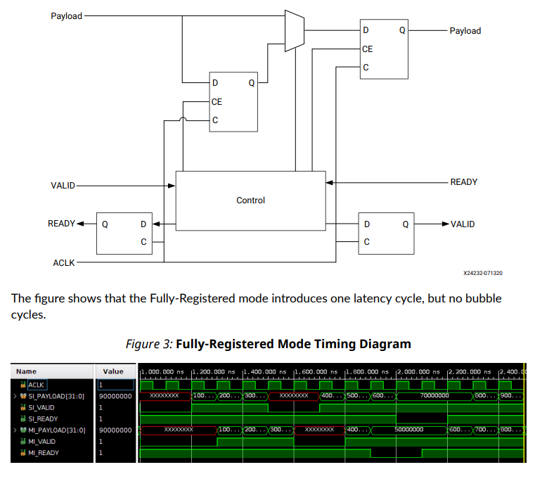
There are two types of register slices. Light-weight with 1 cycle latency and 50% channel utilization and fully registered that has same 1 cycle latency but does not suffer from 50% channel utilization. Light-weight register slice is commonly used for AW/AR/B channels.

A fully-registered register slice implements two deep storage. This improves utilization but suffers from bigger area usage because requires twice the number of flip-flops.
If no data is stored in intermediate flip-flop then data is forwarded to output directly from input. If the output is currently busy then input is registered into an intermediate flip-flop and then output is finally free, data from an intermediate flip-flop is transferred to the output flip-flop. This way no bubble cycle is required and 100% channel utilization can be achieved. For this reason, it is commonly used for W/R channels.
Clock crossing
One of the benefits of using AXI4 as your System-on-chip bus is that for clock crossing simple asynchronous FIFOs can be used. It is common for SoCs to have multiple clock domains. AXI4 was specifically designed with clock crossing and register slicing in mind.

It is reasonable to get 2-4 cycles latency relative to the slowest clock. More sync stages reduce chances of metastability but also increase latency. Careful consideration needs to be done to ensure that both the time-to-failure is reasonable to the lifetime of the product and the latency penalty is reasonable.
In conclusion
AXI4 is one of the best bus protocols. It takes into consideration all the issues with AXI3 and further improves over simple CPU interfaces.
If this article will gain popularity, I will release part two explaining typical designs of:
crossbar
exclusive monitor
data width converter
AXI4 -> AXI4 Lite converter
AXI4 BRAM controller
And many more!
If you have some interesting topics (Like how to synthesize your digital IC, or how to design your own analog IP) you would like for me to cover, feel free to contact me using dialogs or comments.
The source code for this article can be found here.
About author

I am Arman Avetisyan (Twitter, GitHub), and I graduated VLSI IC Design at Synopsys University. I was working for about 3 years designing and verifying Digital IP using Verilog. I wanted to write some articles and share my knowledge because I can see that there are almost no articles covering VLSI Design.
I am open for hire to work on your next-generation Digital IP in Armenia/CIS/US/Canada/EU or remotely. Here is why I think you should hire me:
I designed and verified Avalon-MM SDR SDRAM controller.
I designed, verified and tested over air, mixed software/FPGA radio transceivers (Mono-carrier QPSK RRS filtered, GFSK/GMSK).
I am designing and verifying ArmleoCPU as a hobby project. ArmleoCPU is RISC-V CPU implementing RV32IMA and AXI4. This core includes a Memory management unit, Write-through cache, TLB, Multiplication/division and implements SMP. The repository also includes AXI4 peripherals (UART, SPI, Timer, Core Local Interrupter, Platform Level Interrupt Controller, Multi-channel QSPI Flash/PSRAM/Custom protocol) that will be used to tape out fully custom SoC that can boot and run Linux.
I designed and verified multiple protocol converters.
I also worked on USB3 MAC implementation and I am familiar with Wishbone/Avalon/Ethernet/PCIe/JTAG/USB2/3/4 specifications, CDC/RDC, DFT, RTL-to-GDS flow, IP verification, formal IP verification.
I have a Bachelor's degree in VLSI Integrated Circuit design from Synopsys, NPUA and I am currently pursuing Master's degree in the same specialty.
My experience also includes designing mixed-signal IP, PCB design, Software (C++/C), Firmware (STM32, AVR, 8051), and Web development (Node.js, Angular, React).
If you are interested contact me using dialogs or send me an e-mail: arman.avetisyan2000+habr<at>gmail.com
If you want to make more articles into reality or if this article helped you, you can send me a dime using donation alerts.
References
Wavedrom for creating pictures of the waveforms. Paint.NET for simple diagrams and for Draw.io for more complex ones. GTKWave for waveforms from real projects (including ArmleoCPU).
PS: I used Master/Slave terminology because it matches the AXI4 specification. It is recommended to use alternatives like Host/Client or Host/Device to encourage inclusivity.
