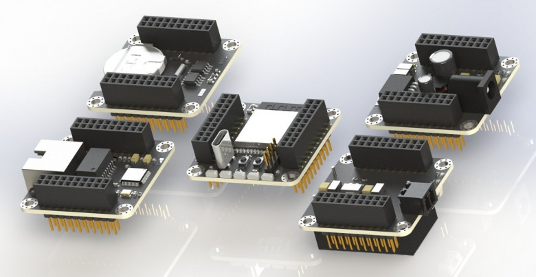
In this article I will talk about my attempt to create flexible, compact and beautiful modular prototyping framework
Circuit design *
Design of electronic circuits
http://GuitarFX.Net Digital (SOFTWARE) modeling of analog guitar distortion, reverb, noise gate etc. effects
The sound of rock music, in particular of hard rock and heavy metal, is largely based on a specially distorted guitar sound, for which electronic “distortion” devices, tube amplifiers in “overloaded” mode, computers with appropriate software and digital processors are used. increasingly using neural network algorithms.
The distorted sound of electric guitars began to gain popularity around the 1960s. Since that time, the sound of overloaded tube amplifiers, connected to powerful dedicated guitar speakers with large dedicated speakers, has been considered the benchmark in rock music. But tube amplifiers were relatively expensive and inconvenient to operate. Therefore, semiconductor distortion devices were developed.
At that time, the electrical circuitry of distortion devices was relatively simple and the signal output from their output only vaguely resembled the sound of an overloaded tube amplifier. Nevertheless, it was still somewhat similar to the “sound of a lamp” and this provided a powerful incentive for designers of analog semiconductor distortion circuits to continue their research, complicate circuits and propose new circuit solutions. The heyday of analog solid-state distortion was around 1995-2010. The most popular were electrical circuit diagrams like those shown in the figure below.
Turning a typewriter into a Linux terminal
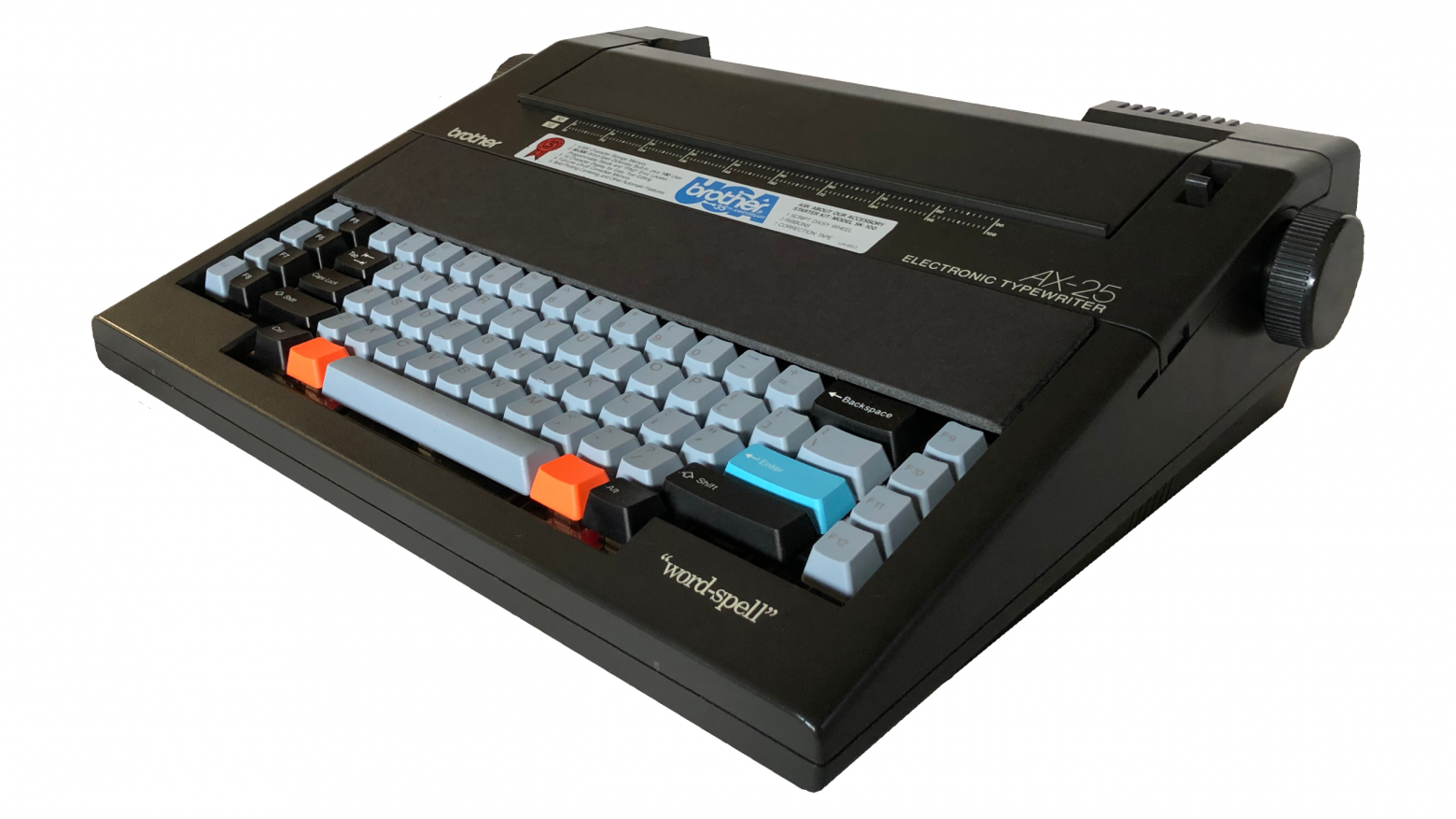
Hi everyone, a few months ago I got a Brother AX-25, and since then, I've been working on turning it into a computer. It uses an Arduino to scan the custom mechanical keyboard and control the typewriter, and a Raspberry Pi is connected to the Arduino over serial so I can log into it in headless mode.
Android for electronics design engineers
There is a list of well-known electronics design tools for Android which can be found in every review for the last 10 years: “Electrodoc”, “Every Circuit”, “Droid Tesla”, “Electronics Toolbox”, “RF & Microwave Toolbox” and so on. Also, there is a lot of trash on the market that turns finding a good tool into a quest.
This short review is about an unknown but cool tool “Circuit Calculator” working on Android devices and intended for professional electronics designers.
The Dino game from Google Chrome using FPGA
Many people are familiar with the situation when there is no Internet, and a small dinosaur appears on the Google Chrome screen. Today we will tell you how to implement this game on the Cyclone IV FPGA board.
We are Yegor Blinov, Egor Kuziakov, and Inga Ezhova - the first-year students of Innopolis University. In our program, there was a course "Computer Architecture", where we had labs with FPGA boards Cyclone IV and MAX10. We were inspired by this equipment and decided to implement the project on one of the boards.
SEPIC-Ćuk split-rail converter average model
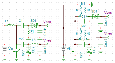
SEPIC-Ćuk split-rail converter can be used to make positive and negative supplies from a single input voltage for relatively well-matched loads like operational amplifiers.
Transient models are time consuming. Average models reduce modeling time drastically.
The PWM switch average models for current- and voltage-mode are described in details in Christophe Basso’s book “Switch-Mode Power Supplies, Second Edition: SPICE Simulations and Practical Designs”. Using of these models for SEPIC and Ćuk converters is also shown.
This text shows how to use the PWM switch average model to design a split-rail SEPIC-Ćuk converter.
A note on small-signal modeling of SEPIC CM CCM
Knowing parameters of small-signal control-to-output transfer functions makes it easier for engineers to design compensation networks of DC/DC converters. The equations for SEPIC can be found in different works and Application Notes, but there are differences. A work has been done to solve this problem.
Simplified design equations for SEPIC with Current Mode control (CM) in Continuous Conduction Mode (CCM) suitable for practical design of compensation networks are shown.
System-on-Chip bus: AXI4 simplified and explained
Protocol AXI4 was developed for High-bandwidth and low latency applications. It is designed to allow communication between master and slave devices. Master is typically a DMA or CPU and slaves are DRAM controllers, or other specific protocol controllers: UART, SPI, and others. Sometimes one component can implement multiple instances of this protocol. Usually, a prefix is used to differentiate between multiple AXI4 interfaces.
For example, Ethernet MAC can integrate DMA and slave interface used to command MAC. MAC can accept commands on the slave interface that contain data about the location of the next ethernet packet and MAC can start fetching this packet using the separate master interface instance.
This article was motivated by common design mistakes AXI4 designers make when they are designing their Digital IP. (Looking at you Xilinx)
DSO138 upgrade
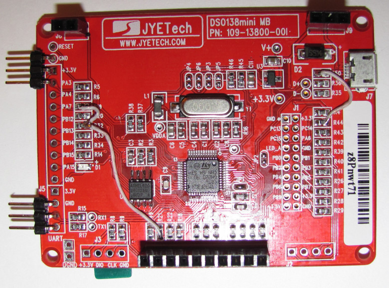
On Ali, an interesting toy – an oscilloscope called DSO138 is sold for a very inexpensive price. It has already gained quite a lot of popularity among electronics lovers, but the parameters of this device, alas, allow it to be more or less fully used only for debugging very low-frequency circuits. Actually, it is not positioned as a tool, but rather as a DIY-kit for novice electronics engineers.
This "toy" oscilloscope is assembled on the STM32F103 microcontroller, and with a fairly competent circuit design of the digital part, the presence of a fairly decent 320X240-dot color display, and not the most rotten analog path, everything, alas, is ruined by very weak ADCs on board the 32F103. The claimed band of 200 kHz can be recognized as such only with a very large stretch. Yes, it will show the presence or absence of a signal with such a frequency, but it will not be possible to really look at something beyond this.
At the same time, the 103-series has a slightly more powerful brother - the STM32F303, it is almost completely compatible with the legs, but it is significantly better in terms of the parameters we are interested in, there are 4 ADCs on board with a conversion frequency of 5 MHz (6 MHz with a 10-bit resolution). In this scenario, if you use all 4 ADCs in parallel with a 10-bit resolution, you can get a effective resolution of up to an honest 24 MSPS (millions of samples per second). The microcontroller is also inexpensive; you can easily find it on the same Ali for very reasonable money again. It is clear that the idea to change the microcontroller arose almost immediately after I tried this DSO138.
At the same time, if upgraded the toy can turn out to be a completely full-fledged tool that even professionals, not just novice amateurs, could already use. With these thoughts in mind, I decided to try to do something with a Chinese toy in my free time.
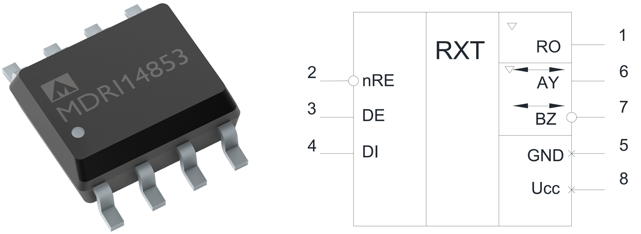
RS485 — a standard for industrial networks. What are the main features of the transceiver microcircuit?
When building a network for communication between a large number of devices, one may think: what interface to choose? Each interface has its own pros and cons that determine its application: CAN — Automotive, RS485 / RS232 — Industrial, Ethernet — Consumer Electronics / Server. What features of the transceiver microcircuit help to protect against many problems during installation and operation? How is the process of measuring and researching of transceiver microcircuits going on? New RS485 microcircuit is ready to get to market!
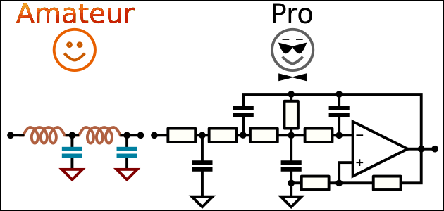
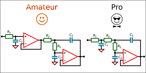
4th Order Low-pass Filter with 1 Op Amp
The idea to build a 4th order low-pass filter looks simple: add one more feedback loop. But there are pitfalls, as always.
Gyrators
Gyrators are impedance converters usually used to simulate inductance in circuits. Though they are rarely used in discrete electronics, they are interesting circuits looking like pole dancers in pictures. There are studies on gyrators, but still something is missing, so it is interesting to do another one.
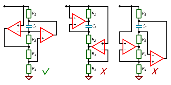
3rd Order Low-pass Filter with 1 Op Amp
Common approach to build a 3rd order low-pass filter is to use two circuit stages and two Op Amps. Making a good One Op Amp design is not always easy, but it is possible.
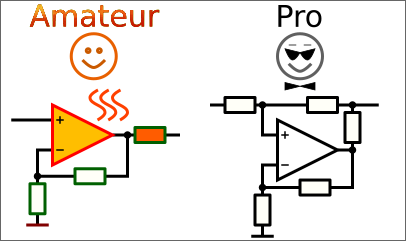
Active Termination Drivers
The easiest way to build a driver with specified output impedance is to use an amplifier with high load compatibility and add a resistor to its output. The penalty is a voltage drop across this resistor, so there is power loss and we need a higher supply voltage. If our driver is able to deliver the same voltage and current to the same load, but the extra resistor will have a lower value, our device will be able to deliver the same output power at a lower supply voltage. Less power losses, less heat, and longer working time when a battery is used.
There is an idea how to solve this problem: active termination. We can synthesize the output impedance!
Now when we know what we want, go to design our drivers!
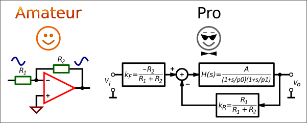
Compensation for Error Caused by Limited Gain-Bandwidth of Operational Amplifiers in Low-pass Filters
An operational amplifier has the internal compensation circuit for stability which limits its working bandwidth. Frequency response of the compensated Op Amp has slope of −6 dB/octave or −20 dB/decade. Unity gain frequency defines the bandwidth where the Op Amp is able to amplify a signal. If we multiply the gain and frequency at any point, the result is the same, allowing us to use this parameter to select the appropriate Op Amp. It is called Gain-Bandwidth Product, GBW or GBP. The limited open-loop gain introduces a closed-loop gain and phase error.
But we want to optimize our circuits, right?
Common misconceptions about space-grade integrated circuits
Space exploration was always fascinating, and recent developments have reignited the interest to the heights never seen since the last man stood on the Moon. People argue about Mars exploration and features of spaceships as their grandparents would’ve done if the internet existed fifty years ago. I’m an electronics engineer working in the aerospace industry, so I know a thing or two about the technical background of this stuff — and I see that these things aren’t common knowledge, and people often have significantly skewed ideas about the reasons behind many things and decisions. Namely, I’d love to speak of some misconceptions about radiation hardened integrated circuits and the means of protection from radiation-induced damage.
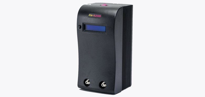
Reverse engineering a high-end soldering station
(This is the translation of the original article performed by baragol)
We had a bunch of photographs of the main PCB, a YouTube video with drain-voltage waveforms of MOSFETs, a forum post with a breakdown of the capacitance values of LC circuit capacitors and also a number of unboxing videos showing the heating-up of the soldering tip. The only thing that really worried me was the video with the measurement of the peak power consumption during the heating-up. There is nothing in the world more helpless and irresponsible and depraved than burned cartridge newly bought for 60 bucks from Amazon. But let me start from the beginning.
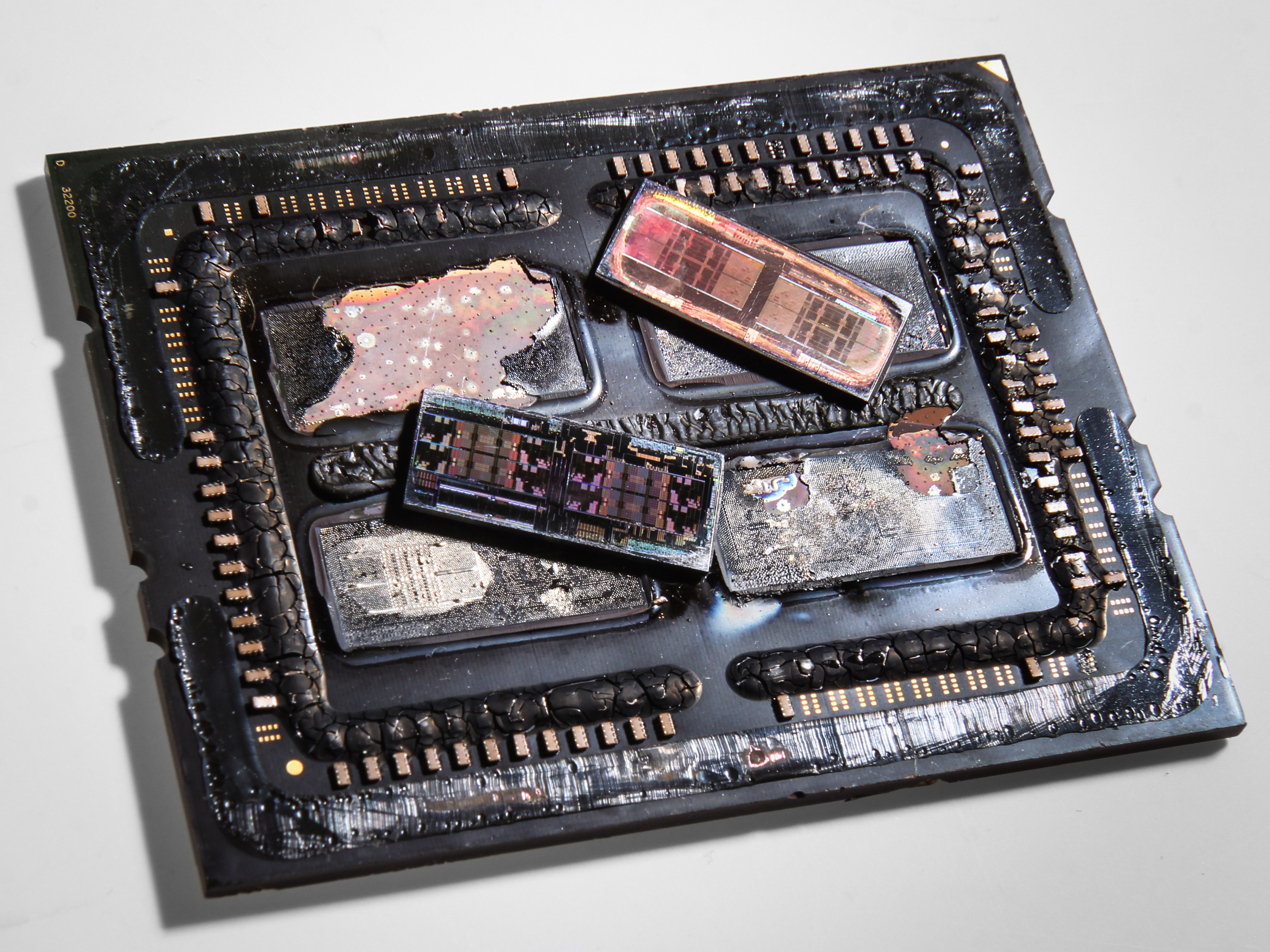
System in Package, or What's Under Chip Package Cover?
Disclaimer: This article is a slightly updated translation of my own piece published on this very site here. If you're Russian-speaking, you may want to check the original. If you're English-speaking, it's worth noting that English is not my native language, so I'll be very grateful for the feedback if you find something weird in the text.
Authors' contribution
MaFrance351 2117.0dlinyj 1714.0Lunathecat 1683.0dmitriyrudnev 1673.0amartology 1314.0OldFashionedEngineer 902.0the_bat 776.0ynoxinul 744.0zatim 544.0MyElectronix 480.0